Pololu VL53L7CX Time-of-Flight 8×8-Zone Wide FOV Distance Sensor Carrier with Voltage Regulator - 350cm Max
Price:
Sale price
£18.90
Stock:
Quantity:
 Skip to content
Cart
Your cart is empty


This Pololu sensor is a carrier/breakout board for ST’s VL53L7CX laser-ranging sensor, which offers fast and accurate ranging up to 3.5 m through a digital I²C interface.
It has an extra-wide 60°×60° square field of view (FOV) (90° diagonal), and it can measure absolute distances to multiple targets simultaneously across multiple zones, providing enough data for a depth map with up to 8×8 resolution.
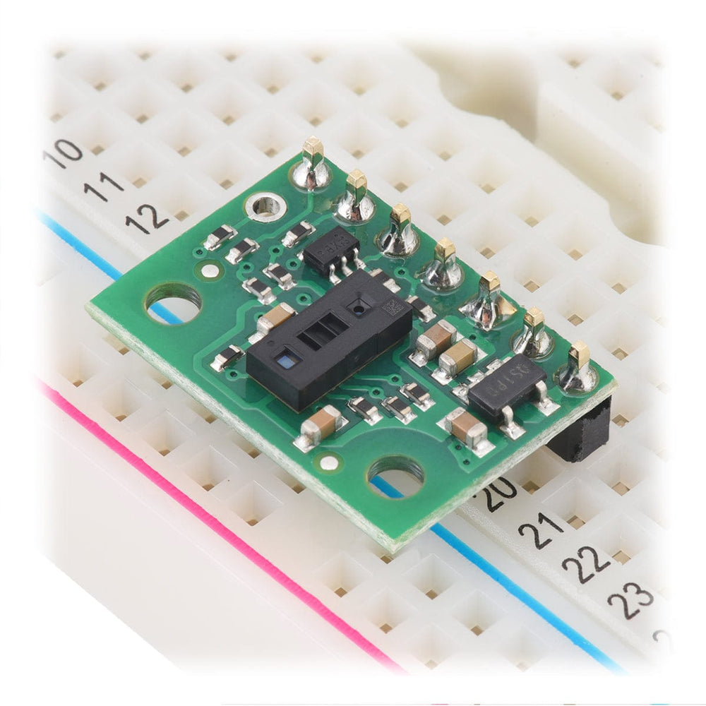
The board includes a 3.3 V linear regulator and level-shifters that allow it to work over an input voltage range of 2.5 V to 5.5 V, and the 0.1″ pin spacing makes it easy to use with standard solderless breadboards and 0.1″ perfboards.
Note: This is not recommended for use with 8-bit MCUs; for such applications, consider the VL53L1X, VL53L0X carrier, or VL6180X carrier.
The VL53L7CX from ST Microelectronics is a long-distance, ranging time-of-flight (TOF) sensor integrated into a compact module. This board is a carrier for the VL53L7CX, so we recommend careful reading of the VL53L7CX datasheet before using this product.
The VL53L7CX is effectively a tiny, self-contained lidar system featuring an integrated 940 nm Class 1 laser, which is invisible and eye-safe. Unlike conventional IR sensors that use the intensity of reflected light to estimate the distance to an object, the VL53L7CX uses ST’s FlightSense technology to precisely measure how long it takes for emitted pulses of infrared laser light to reach the objects and be reflected back to a detector. This approach ensures absolute distance measurements independent of ambient lighting conditions and target characteristics (e.g. color, shape, texture, and reflectivity), though these external conditions do affect the maximum range of the sensor.
The VL53L7CX is distinguished from ST’s previous time-of-flight sensors by its extra-wide 60°×60° square field of view (FOV), which allows for a 90° FOV across the diagonal, and its multi-zone ranging output. Its field of view is divided into a number of zones, configurable as a 4×4 or 8×8 grid, and the sensor provides separate readings for each zone (which can include multiple targets per zone). This effectively makes the VL53L7CX a basic 3D lidar, since instead of measuring only a single distance (1D lidar), it can provide enough data to generate a low-resolution depth map of the environment within its field of view.
Under favorable conditions, the sensor can report distances up to 3.5 m (11 ft) with 1 mm resolution. The minimum ranging distance is 20 mm. Ranging measurements are available through the sensor’s I²C (TWI) interface, which is also used to configure sensor settings, and the sensor provides three additional pins: an interrupt output and two inputs to disable and reset the I²C interface.
The VL53L7CX is a great IC, but its small, leadless, LGA package makes it difficult for the typical student or hobbyist to use. It also operates at a recommended voltage of 2.8 V to 3.3 V, which can make interfacing difficult for microcontrollers operating at 5 V. Our breakout board addresses these issues, making it easier to get started using the sensor, while keeping the overall size as small as possible.
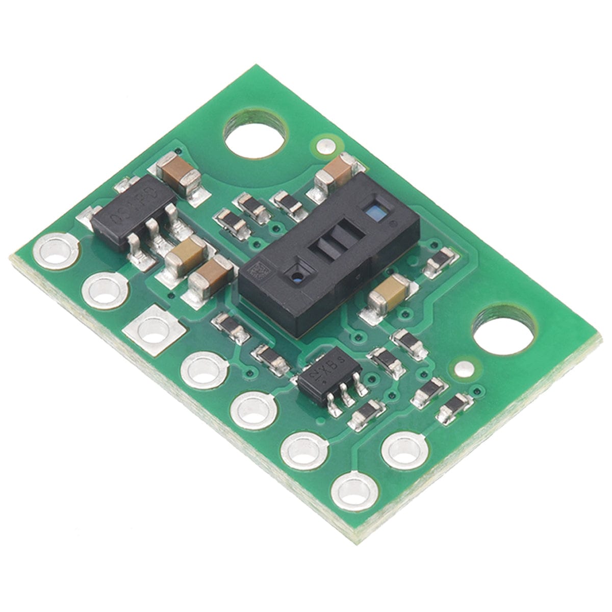
The carrier board includes a low-dropout linear voltage regulator that provides the 3.3 V required by the VL53L7CX and allows the sensor to be powered from a 2.5 V to 5.5 V supply. The regulator output is available on the VDD pin and can supply around 100 mA to external devices. The breakout board also includes a circuit that shifts the I²C clock and data lines to the same logic voltage level as the supplied VIN, making it simple to interface the board with 5 V systems, and the board’s 0.1″ pin spacing makes it easy to use with standard solderless breadboards and 0.1″ perfboards. The board ships fully populated with its SMD components, including the VL53L7CX.
Important note: This product might ship with a protective liner covering the sensor IC. The liner must be removed for proper sensing performance.

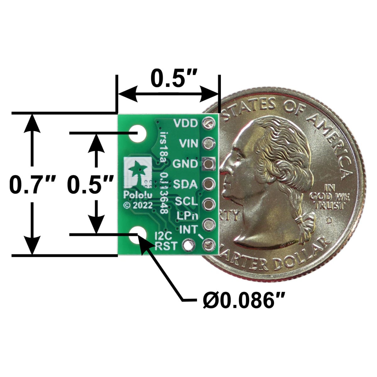
At least four connections are necessary to use the VL53L7CX board: VIN, GND, SCL, and SDA. The VIN pin should be connected to a 3.3 V to 5.5 V source, and GND should be connected to 0 volts. An on-board linear voltage regulator converts VIN to a 3.3 V supply, which can be accessed via the VDD pin, for the VL53L7CX IC. Supply voltages between 2.5 V and 3.6 V can also be connected to VDD (with VIN left disconnected) to bypass the regulator and power the board directly.
The I²C pins, SCL and SDA, are connected to built-in level-shifters that make them safe to use at voltages above VDD; they should be connected to an I²C bus operating at the same logic level as VIN (or VDD, if powering the board through VDD).
The LPn and I2C_RST pins are inputs and the INT pin is an open-drain output. LPn and INT are pulled up to VDD by the board, while I2C_RST is pulled down to GND. These three pins are not connected to level-shifters on the board and are not 5V-tolerant, but LPn and INT are usable as-is with 5 V microcontrollers: the microcontroller can read the INT output as long as its logic high threshold is below VDD, and the microcontroller can alternate its own output between low and high-impedance states to drive the LPn pin. Alternatively, our 4-channel bidirectional logic level shifter can be used externally with those pins.

| Pin | Description |
| VDD | Regulated 3.3 V output. Up to around 100 mA is available to power external components. (If you want to bypass the internal regulator, you can instead use this pin as an input for voltages between 2.5 V and 3.6 V with VIN disconnected.) |
| VIN | This is the main 3.3 V to 5.5 V power supply connection. The SCL and SDA level shifters pull the I²C lines high to this level. |
| GND | The ground (0 V) connection for your power supply. Your I²C control source must also share a common ground with this board. |
| SDA | Level-shifted I²C data line: HIGH is VIN, LOW is 0 V |
| SCL | Level-shifted I²C clock line: HIGH is VIN, LOW is 0 V |
| LPn | This pin is an active-low I²C disable input; the board pulls it up to VDD to enable I²C communication by default. Driving this pin low disables I²C communication (typically used as part of a process to change I²C addresses). This input is not level-shifted. |
| INT | Programmable interrupt output (VDD logic level). This output is not level-shifted. |
| I2C_RST | This pin is an active-high I²C reset input; the board pulls it down to GND by default. Driving this pin high resets the I²C interface (but not the entire sensor). This input is not level-shifted. |
The VL53L7CX can be configured and its distance readings can be queried through the I²C bus. Level shifters on the I²C clock (SCL) and data (SDA) lines enable I²C communication with microcontrollers operating at the same voltage as VIN (2.5 V to 5.5 V). A detailed explanation of the I²C interface on the VL53L7CX can be found in its datasheet, and more detailed information about I²C in general can be found in NXP’s I²C-bus specification.
The sensor’s 7-bit target address defaults to 0101001b on power-up. It can be changed to another value by writing one of the device configuration registers, but the new address only applies until the sensor is reset or powered off. ST’s UM3038 document describes how to use multiple VL53L7CX sensors on the same I²C bus by individually enabling I²C communication on each sensor with its LPn pin and assigning it a unique address.
The I²C interface on the VL53L7CX is compliant with the I²C fast mode plus (1 MHz) standard.
In contrast with the information available for many other devices, ST has not publicly released a register map and descriptions or other documentation about configuring and controlling the VL53L7CX. Instead, communication with the sensor is intended to be done through ST’s VL53L7CX ULD API (STSW-IMG036), a set of C functions that take care of the low-level interfacing. To use the VL53L7CX, you can customize the API to run on a host platform of your choice using the information in the API documentation. Alternatively, it is possible to use the API source code as a guide for your own implementation.
The VL53L7CX API appears to be functionally identical to the VL53L5CX API, so if you want to use the VL53L7CX with an Arduino-compatible controller, you can try SparkFun’s VL53L5CX Arduino library, a port of ST’s API that works with the Arduino platform. To install it, search for “SparkFun VL53L5CX” in the Arduino Library Manager. (Note: 8-bit microcontrollers, including that of the Arduino Uno, typically do not have enough RAM or program memory to use with the VL53L7CX, so this library is mainly useful for more powerful MCUs like a 32-bit RP2040 or ESP32.)
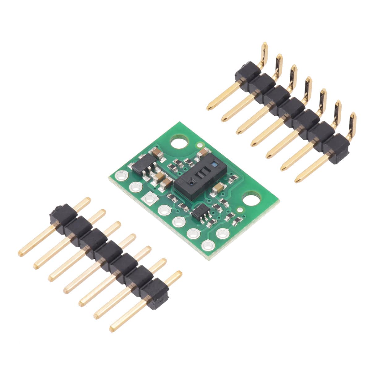
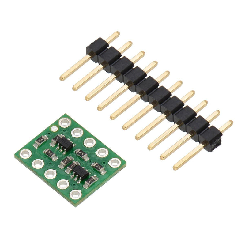
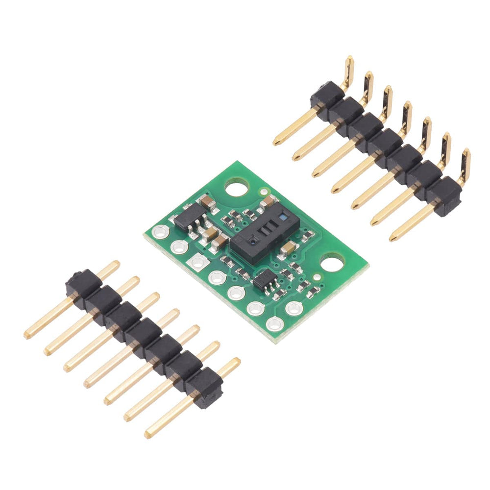
Along with the VL53L7CX board, a 1×8 strip of 0.1″ header pins and a 1×7 strip of 0.1″ right-angle header pins are included.
You can solder the header strip of your choice to the board for use with custom cables or solderless breadboards, or you can solder wires directly to the board itself for more compact installations.
Your payment information is processed securely. We do not store credit card details nor have access to your credit card information.